
Ask an FPGA design engineer about securing their designs and a typical reply is likely “Oh – we don’t have to worry about that, our FPGA vendor takes care of silicon security”. This perspective is partially true in that FPGA vendors provide security functionality to protect a user’s bitstream and the design data that uniquely programs an FPGA against copying, cloning, and reverse engineering. Some FPGA vendors are now also offering more advanced security features. For example, Xilinx’s latest devices, such as the Zynq UltraScale+ MPSoC, now include a Hardware Root of Trust, as well as hardware encryption with built-in countermeasures against Differential Power Analysis (DPA) attacks.

Processor Features in the Xilinx Zynq UltraScale+ MPSoC (Courtesy of Xilinx)
But what about securing the unique logic designs that are implemented by design engineers inside an FPGA? This is clearly the responsibility of the FPGA designers to ensure that no security vulnerabilities exist once their end products are shipped to customers.
Is Security Verification Necessary in an FPGA?
In the new era of big data analytics and machine learning, the value of information is skyrocketing. Hackers are now incentivized to acquire any and all information about the way people live and companies operate. Data that was once considered of little value and not worth the effort to acquire is suddenly creating significant revenue streams for cybercriminals. As the “cyber attack surface” expands in the connected world of the IoT, it is now expected by your customers that your products will be protected against hackers trying to obtain assets such as personal, health, financial, and operational information. In addition, your customers also expect that your FPGA designs cannot be manipulated or remotely controlled to cause disruption, denial of service, or allow inappropriate access to restricted corporate systems and datacenters.
The need to secure FPGA designs is thus no longer optional. Implementing a Design-For- Security (DFS) methodology within an RTL design process is the most efficient and cost effective method to verify that your FPGA designs are free of security vulnerabilities.
DFS for FPGAs
There are several key business values for performing DFS for FPGAs. Specifically, it provides FPGA designers with:
- Accountability: Threat model is defined and enforced from architecture to bitstream
- Predictability: Schedule, cost, and manpower are proactively planned and managed
- Sales Enablement: Improved company branding and product value by ensuring FPGA security
In order to implement DFS, there are two key steps 1) threat modeling and 2) security verification. DFS begins during the architecture phase of the FPGA design process with the creation of a threat model. Threat modeling has become an integral part of the design specification process at many major corporations such as Microsoft (Security Development Lifecycle) [1] and Intel (Product Security Practices) [2] . Threat modeling is composed of three key components: 1) Acknowledging that FPGA designs have assets of value worth protecting (e.g. encryption keys or proprietary firmware), 2) recognizing internal and external threats that can exploit vulnerabilities in order to cause damage to these assets, and 3) utilizing the appropriate countermeasures needed to prevent or mitigate said threats.
Threat Modeling is a procedure for optimizing silicon security by identifying assets and vulnerabilities, and then defining countermeasures to prevent, or mitigate the effects of, threats to the system
The second phase of the DFS process is security verification. It is important to understand that there is a significant difference between verifying functionality and verifying security. The engineering skills and tools needed for one cannot be easily applied to the other. Verifying security is an intricate process made easier by DFS and security-specific languages such as Sentinel™ from Tortuga Logic reduce the time and skills required to perform security verification across formal verification, simulation, or emulation. Using an intuitive security language like Sentinel™ allows the FPGA verification engineer to complete security verification of their RTL design and embedded SW in a few days instead of many months.
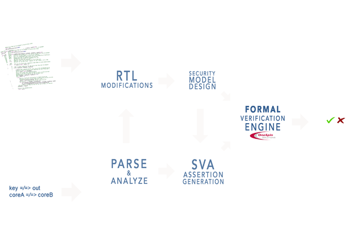
Security verification platforms exist to provide a convenient workspace for verifying FPGA designs. Shown below is the Tortuga Logic Prospect™ security verification platform for the Sentinel™ language. Please note that the FPGA designer’s RTL is only modified to create a security model for verification – the original RTL source is maintained for logic synthesis, timing analysis, and functional verification.
The results of executing the security properties developed as part of the threat modeling are the detection and location of any existing security vulnerabilities. Verification runtimes typically vary from 30 minutes to a couple of hours for multi-million gate equivalent FPGA designs. As you prepare to release your FPGA design with a completed FPGA security verification, you will have the confidence that all security threats have been assessed and documented. In addition, countermeasures and architectural features were created and verified to mitigate vulnerabilities. The end result is an increase in the market value of your end product due to the extra steps you have taken to assure FPGA security.
Getting Started with DFS for FPGAs
FPGA security and DFS are relatively new engineering activities and many companies realize they do not have the necessary skills, experience, and tools to implement a DFS process in a timely and cost-effective manner. Tortuga Logic provides Hardware Security Assessment (HSA) services to bootstrap an engineering organization by insourcing security verification knowledge. Tortuga’s security experts work alongside your engineers to develop a threat model for your FPGA design, create the necessary security properties, and then execute verification of the properties. The benefits of an HSA include the delivery of a security report for your FPGA design and a library of Sentinel security properties to serve as a basis for your next project.
Summary
Securing the unique logic design and embedded software of FPGAs has become essential in today’s newly-connected world of billions of devices. Cyber attacks have become increasingly focused on silicon designs such as FPGAs and as hackers improve their techniques across a fast-growing attack surface, so do their success rates. It is important to adopt a Design-for-Security methodology for FPGA designs in order to mitigate the risk of threats and ensure your security review has both accountability and predictability. More importantly, DFS helps to increase the value of your products.
About Jason Oberg
Dr. Oberg is one of the co-founders and Chief Executive Officer of Tortuga Logic. He oversees technology and strategic positioning of the company. He is the founding technologist of the company and has brought years of intellectual property into the company that he successfully transferred out of the University of California. Dr. Oberg is leading the company to meet all milestones including raising capital, tripling the team size, putting together strategic partnerships, and generating revenue on all products and services. Dr. Oberg has a B.S. degree in Computer Engineering from the University of California, Santa Barbara and M.S. and Ph.D. degrees in Computer Science from the University of California, San Diego.
References
1. Microsoft Website: Microsoft Security Development Lifecycle: https://www.microsoft.com/en-us/sdl/
2. Intel Website: Intel Security Product Security Practices: https://www.mcafee.com/us/resources/misc/ms-product-software-security-practices.pdf
3. Tech Talks: Five Domains Where IoT Security Needs to be Addressed: https://bdtechtalks.com/2015/11/04/5-domains-where-iot-security-needs-to-be-addressed/comment-page-1/