
It’s the natural inclination of engineering management to address difficult and new issues in product development by testing for them late in the design cycle. Often the new issues are not well understood, EDA tools and techniques to address the issues are new and unproven (if available at all), and design engineers have little or no experience in the subject matter so they are still in a learning phase. Let’s face it, any change is difficult for engineering teams as it can introduce risk, typically results in dreaded schedule delays, and engineering budgets weren’t funded adequately to allow for purchasing new solutions and adding headcount. So engineering management usually takes the path of least resistance and attempts to test for security vulnerabilities late in the design cycle instead of designing-for-security from the start of the RTL design process.
History repeats itself. As the size and complexity of ASICs grew quickly in the 1990s, we saw “design-for-test” (DFT) become a mandate for ASIC design teams to address the difficulty in achieving adequate test coverage. As semiconductor process technologies dramatically shrank in the early 2000s, we witnessed “design-for-manufacturing” (DFM) tools and methodologies quickly adopted by the back-end of SoC design teams to address yield problems during silicon manufacturing. So it should come as no surprise to learn that “design-for-security” (DFS) is the latest capability that “should be added to the RTL design flow” due to the need to secure silicon in a world full of cybercriminals and black-hat hackers.
The motivation for DFS is the same as any other “design-for” capability, it’s all about cost. Whether it’s finding a software bug, a hardware defect, or a security vulnerability, the cost is significantly higher if found later in the product life cycle. The chart below shows the cost to fix a defect which can also be applied to finding security vulnerabilities. What is clear is it is incredibly more expensive to fix defects and security vulnerabilities in the field! The return on investment for adding DFS capability to an RTL flow is thus easy to determine – a single vulnerability can easily cost millions of dollars to correct once a product has shipped. And if you’re thinking “ah, but it’ll never happen to OUR SoC designs”, think again. A recent post [2] on SemiWiki.com reported on just the tip of the iceberg of actual security vulnerabilities discovered in products in 2015. The author correctly posited “Just how many different IoT companies and arenas were breached? The answer might surprise you– not to mention terrify you.”

Intel was one of the first to address silicon security with the publication of a paper describing a Hardware Security Development Lifecycle (HSDL) that was used on commercial CPUs, chipsets, and SoCs [1]. The Intel paper described how a structured flow of analysis and testing activities organized in five phases accelerated the discovery of security issues that could be exploited through software or physical attacks. Tortuga Logic has deployed its DFS solution as shown below in a typical HSDL flow:

DFS begins during the SoC specification and architecture development process with the creation of a library of security properties using the Sentinel™ security language, a language developed specifically by Tortuga Logic to express silicon security properties throughout the entire design lifecycle. The key here is that security properties are documented from the beginning in architectural design and not after the fact. This library of security properties then feeds into the standard verification process from IP block verification to embedded software to SoC integration using the existing EDA tools already in place. At each stage of the SoC verification process, different methodologies are required. Tortuga Logic’s DFS solution allows the library of Sentinel security properties to feed into all stages of the SoC verification process.
Tortuga Logic provides Hardware Security Assessments (HSAs) to assist design teams that are new to the DFS process. Tortuga’s security engineers first work with the silicon design team to scope their design and to reach agreement on a security threat model. Next, Sentinel is used to create the library of security properties. Tortuga customers report realizing significant time savings by using security property libraries provided by Tortuga Logic as compared to developing assertions in general purpose languages such as Perl, TCL, or SVA. In the majority of the cases, it is not even possible to express security properties in these existing languages.
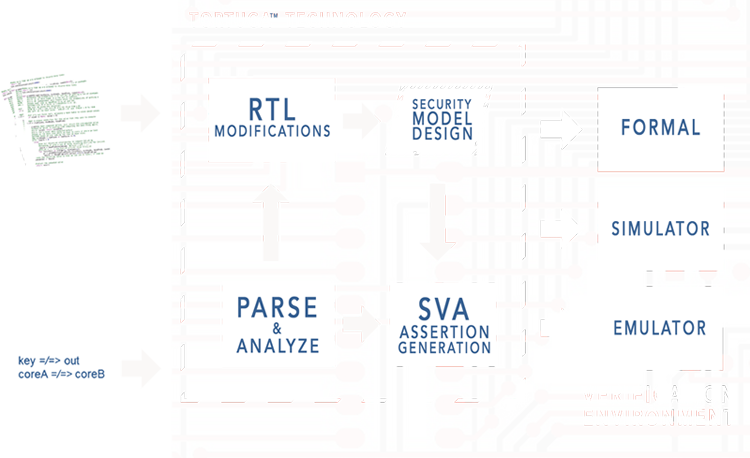
When RTL design work commences, Tortuga’s security verification environment, Prospect™, is used to verify the SoC design using the library of security properties. Currently Prospect is used in conjunction with a formal verification tool. In the future, additional verification platforms will be supported to find vulnerabilities during software/hardware execution and support the entire RTL design flow through tapeout. A view of the Tortuga technology architecture is shown below. It should be noted that the RTL is only modified to create a security model for verification – the original RTL source is maintained for logic synthesis, timing analysis, and functional verification.
Summary
Security vulnerabilities in silicon designs represent huge potential financial losses, not to mention the severe detrimental damage to a company’s brand name. SoC designers currently attempt to test for security vulnerabilities very late in the design cycle, which produces very little discovery and resolution. Tortuga Logic provides a design-for-security (DFS) process that integrates easily into an RTL process and allows for security verification during the entire SoC design process, from architecture development to tapeout.
About Jason Oberg
Dr. Oberg is one of the co-founders and Chief Executive Officer of Tortuga Logic. He oversees technology and strategic positioning of the company. He is the founding technologist of the company and has brought years of intellectual property into the company that he successfully transferred out of the University of California. Dr. Oberg is leading the company to meet all milestones including raising capital, tripling the team size, putting together strategic partnerships, and generating revenue on all products and services. Dr. Oberg has a B.S. degree in Computer Engineering from the University of California, Santa Barbara and M.S. and Ph.D. degrees in Computer Science from the University of California, San Diego.
References
- *Khattri et al.,”HSDL: A Security Development Lifecycle for Hardware Technologies”, 2012 IEEE International Symposium on Hardware-Oriented Security and Trust
- https://www.semiwiki.com/forum/content/5920-whose-iot-devices-were-breached-2015-a.html